Present Research Activities:
| We are working on various aspects of Nanoscience and Nantechnology, in the field of semiconductor nanostructures,
Plasmonics, Carbon Nanotubes, Graphene & MoS2,
Polymeric 2D Organic Semiconductor g-C3N4,
Organic FETs, Perovskite Solar cell and LEDs etc.
|
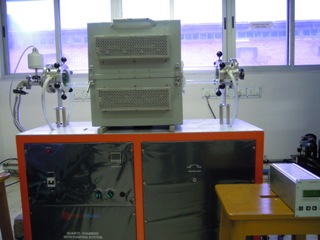
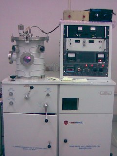
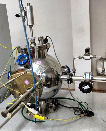
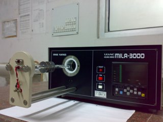
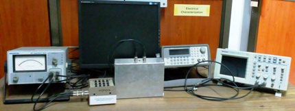
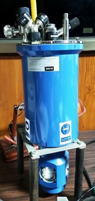
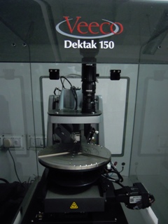
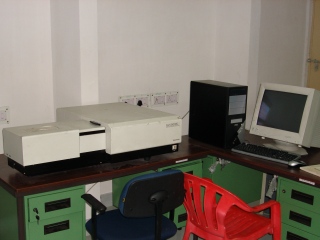
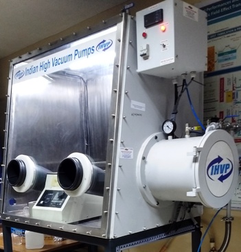
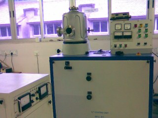
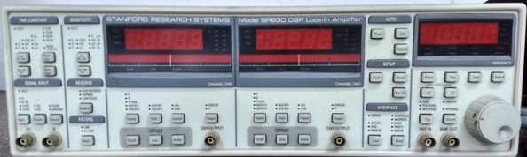
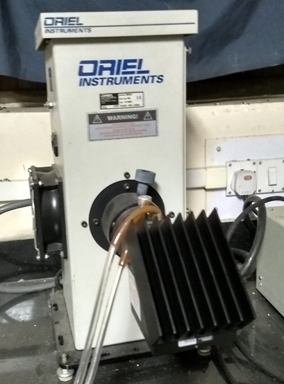
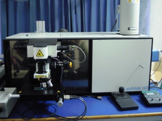
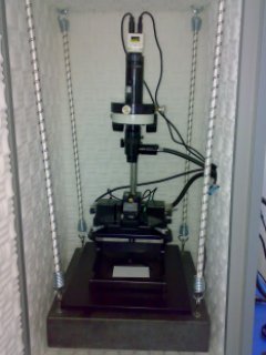
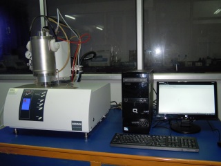
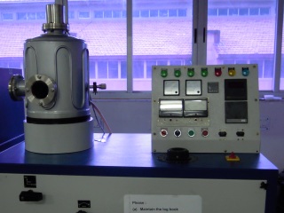
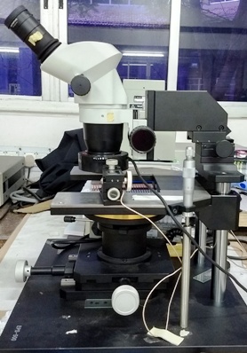
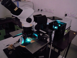
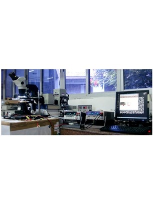
![]() Research Facilities:
Research Facilities:
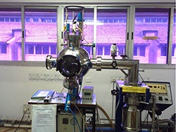
Chemical Vapor Deposition System
Magnetron Sputtering (DC and RF)
PECVD System
Rapid Thermal Annealer
Electrical characterization setup
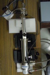
Optical cryostat
Thin film Profilometer
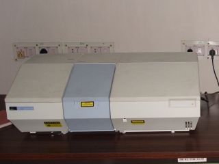
UV-Vis-NIR Spectrophotometer
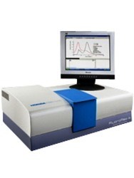
Fluorescence Spectrometer
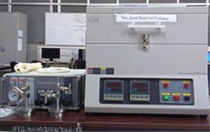
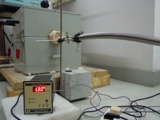
Two-Zone Furnace
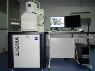
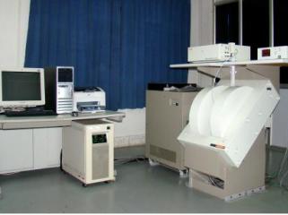
Field Emission SEM
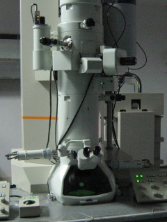
Transmission Electron Microscope
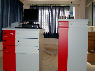
Electron Spin Resonance Spectrometer
Spectroscopic Ellipsometer
|
Thermal Vapor Deposition System
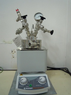
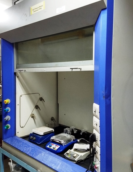
High Pressure Reactor (Autoclave)
Glove box with Spin coater
Electron Beam Evaporation Unit
Lockin Amplifier
High power Xenon lamp+reflector
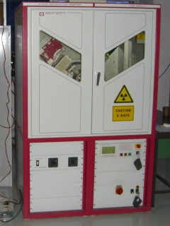
X-Ray Diffractometer
FourierTransform Infrared Spectrometer
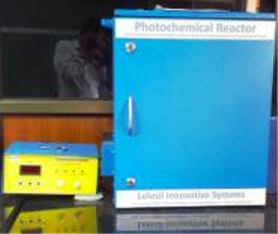
Photochemical Reactor
Magnetron Co-Sputtering (DC+RF)
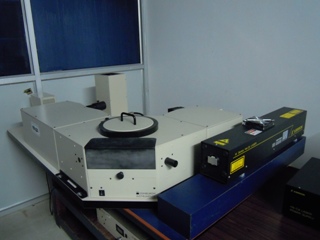
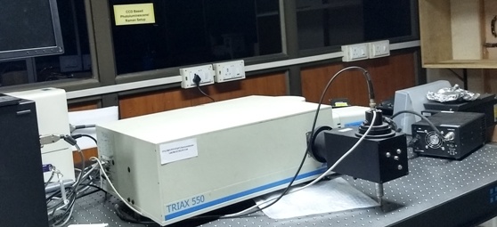
Raman Spectrometer
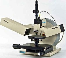
Scanning Probe Microscope
Differential Scanning Calorimeter
|
Thermal Evaporation Unit
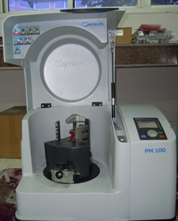
Planetary Ball mill
Fumehood
Laser PL Spectrometer
CCD PL-Raman setup
Micro-probe station
Closed Cycle Helium Cryostat
Photoconductivity Setup
Photo I-V Setup
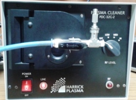
Plasma Cleaner
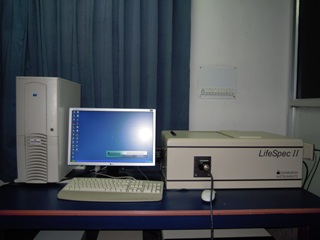
Time-Resolved PL Spectrometer
Vibrating Sample Magnetometer
Superconducting Quantum Interface Device |
|---|